 |
 |
 |
| RU |
|
Login
Newsletters
There is no newsletter category found. Information
|
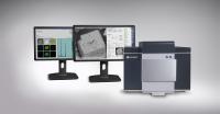
Keysight Technologies Adds Fully Integrated EDS Capabilities to Low-Voltage, High-Resolution FE-SEM System 02/16/2015 Keysight Technologies, Inc. (NYSE: KEYS) announced the immediate availability of its newest field-emission scanning electron microscope (FE-SEM), the 8500B. The technologically advanced Keysight 8500B offers scientists the analytical power of energy dispersive spectroscopy (EDS), fully integrated within a remarkably compact, low-voltage FE-SEM. Keysight designed this easy-to-install, plug-and-play FE-SEM for use in practically any lab and requires only an AC power outlet. The compact 8500B delivers outstanding image resolution rivaling that of much larger and more expensive FE-SEMs. The new 8500B system's fully integrated silicon-drift x-ray detector, digital multichannel analyzer and intuitive software interface put EDS capabilities at researchers' fingertips, allowing them to perform quantitative elemental analysis on arbitrary points, on a continuous line scan or in a user-defined regional map. The Keysight 8500B is capable of detecting elements as light as carbon, up to americium. EDS results are analyzed and displayed in real time and researchers can export the data for further off-line analysis. Keysight's patented event-streamed spectrum imaging saves the full spectrum at every pixel for analysis and display. Dynamic element mapping allows real-time selection or editing of elements and processing parameters during spectrum image collection. The 8500B also offers several low-voltage imaging techniques for enhancing surface contrast and allowing the observation of nanoscale features on a wide variety of nanostructured materials, including polymers, thin films, biomaterials, and other energy-sensitive samples on any substrate, even glass. A novel, compact electrostatic lens and electron beam column design helps guarantee consistent, replicable performance without constant re-tuning of the column. In addition, continuously variable beam energy optimized for low-voltage operation minimizes the need to conductively coat samples when using the Keysight 8500B FE-SEM. A software-controlled, programmable X/Y/Z stage enables simple sample navigation. Company profile: Keysight Technologies Related Information:
Companies' news
KIPiS articles
|
Current issue
Search
|
|
|
| © "Test & Measuring Instruments and Systems" ("KIPiS"), 2000-2024 |


